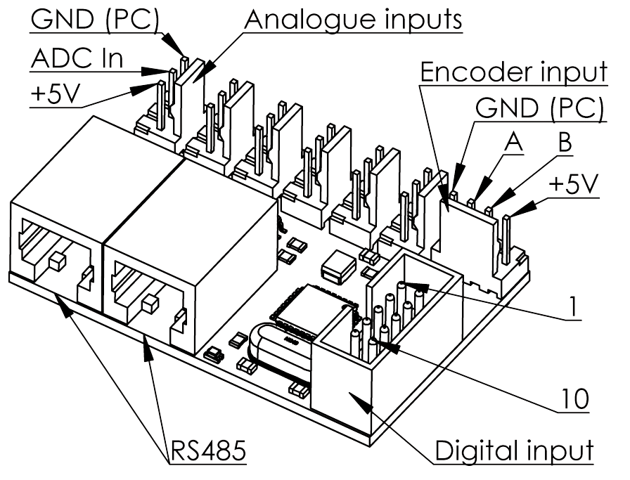
Chapter 13. RS485 modules
These modules were developed to expand the I/O and function capabilities along an RS485 line of the PCI motion control card.
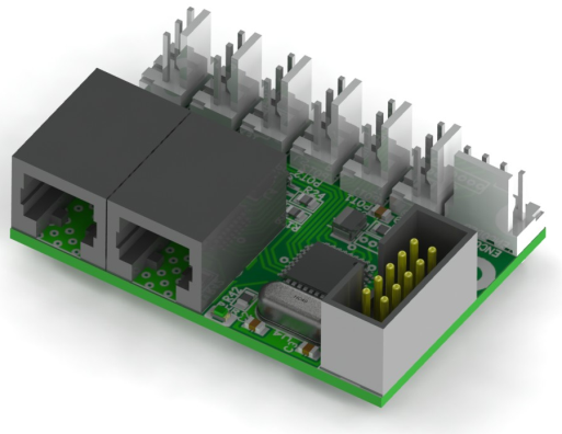
13.1. Available module types
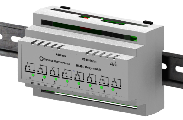
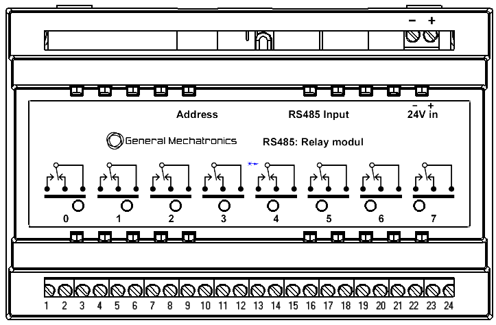
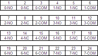
8-channel relay output module
The relay output module provides eight NO-NC relay output on a three pole terminal connector for each channel.
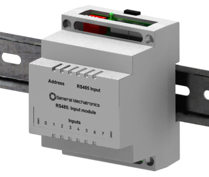
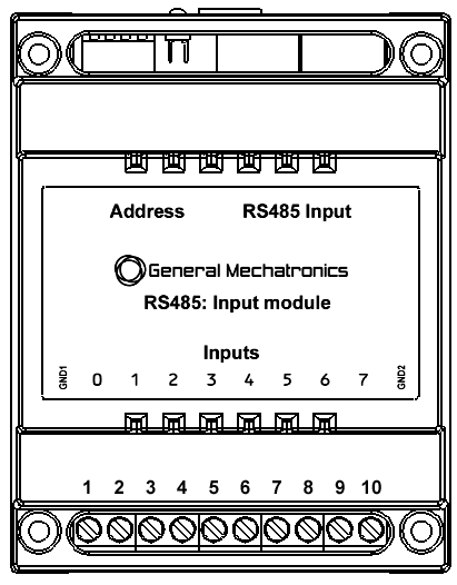
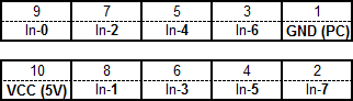
8-channel digital input module
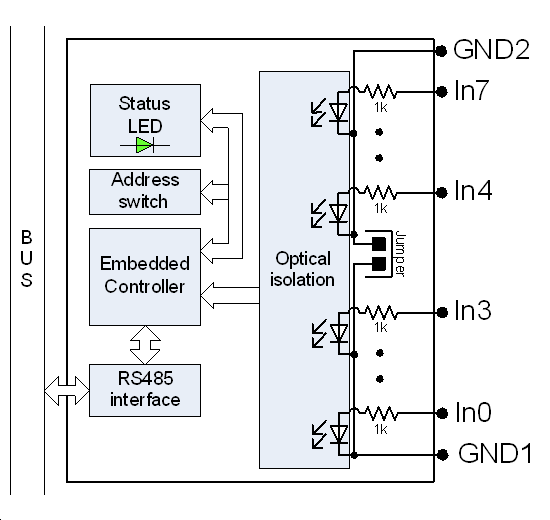
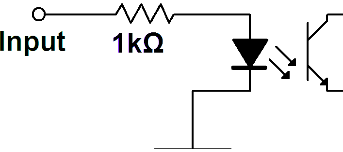
The digital input module provides eight optical isolated digital input pins.
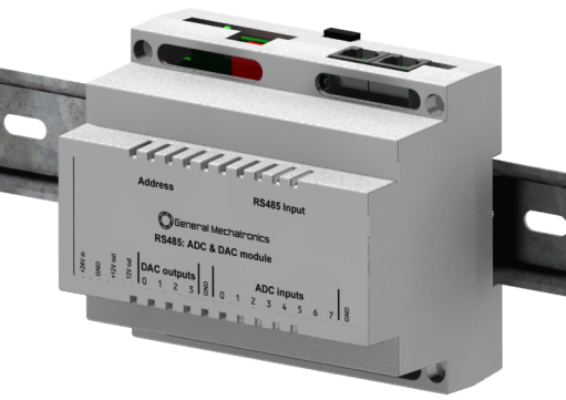
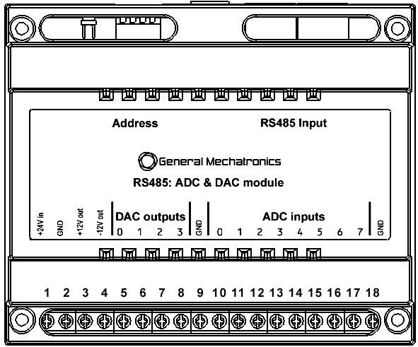
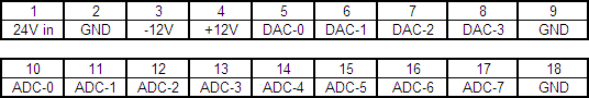
8 channel ADC and 4-channel DAC module
The ADC and DAC module provides four digital-to-analogue converter outputs and eight analogue-to-digital inputs. This module is also optically isolated from the PCI card.
Teach Pendant module
The teach pendant module provides 8 digital input channels for pushbuttons, 6 ADC input channels for joystick or potentiometers and 1 encoder input for a handwheel.
13.2. Automatic node recognizing
Each node connected to the bus is recognized by the PCI card automatically. During starting LinuxCNC, the driver exports pins and parameters of all available modules automatically.
13.3. Fault handling
If a module does not answer regularly the PCI card drops down the module.
If a module with output don’t get data with correct CRC regularly, the module switch to error state (green LED blinking), and turns all outputs to error sate.
13.4. System description
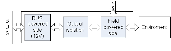
13.4.1. Powering of the nodes
Each module is electronically isolated from the bus, hence they have a bus powered side, and a field powered side.
General bus settings
13.4.2. Connecting of the nodes
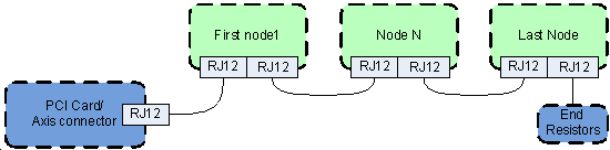
The modules on the bus have to be connected in serial topology, with termination resistors on the end. The start of the topology is the PCI card, and the end is the last module.
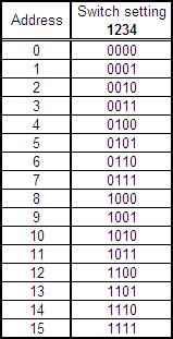
13.4.3. Addressing
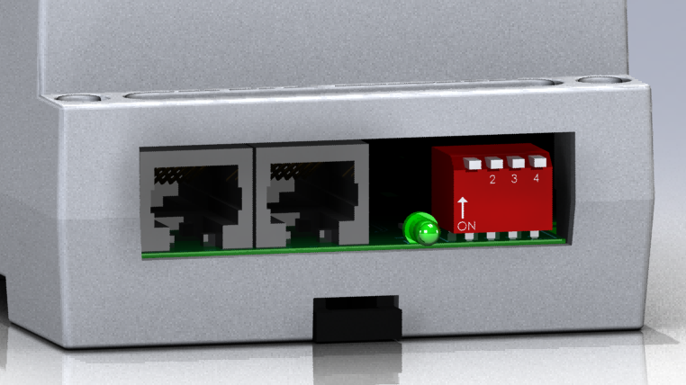
Each node on the bus has a 4 bit unique address that can be set with the red DIP switch.
13.4.4. Status LED
The green LED indicates the status of the module:
Blink, when the module is only powered, but not yet identified, or when the module is dropped down.
Off, during identification (computer is on, but LinuxCNC not started)
On, when it communicates continuously.
13.5. Modules
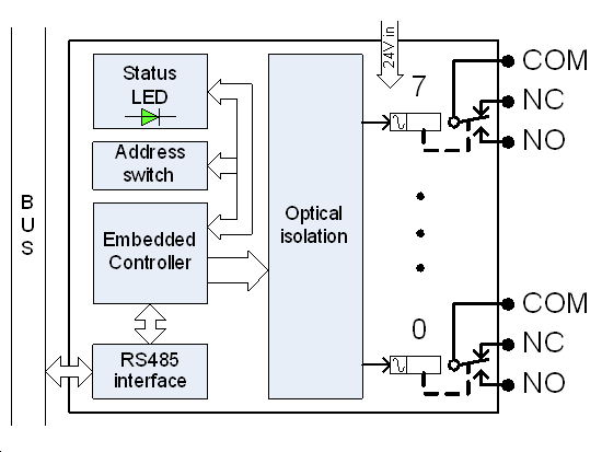
13.5.1. Relay output module
Block diagram
Electrical characteristics
Power:
Bus voltage:12V
Maximum bus power consumption:150mA
Field power voltage:24V
Maximum field power consumption (all relays on):270mA
Insulation:
Optical isolation voltage:2500VRMS
Relay characteristics:
Maximum switching current:10A
Maximum switching AC voltage:250V
Maximum switching DC voltage:30V
Dielectric strength:5000V
Connection
Error state
If a bus error occurs, the module will switch to error state (green LED blinking). And turn off all output relays.
HAL configuration
All the pins and parameters are updated by the following function:
gm.<nr. of card>.rs485
It should be added to servo thread or other thread with larger period to avoid CPU overload.
Every RS485 module pin and parameter name begins as follows:
gm.<nr. of card>.rs485.<modul ID>, where <modul ID> is from 00 to 15.
Pins:
.relay-<0-7>(bit, Out)--Output pin for relay
Parameters:
.invert-relay-<0-7>(bit, R/W)--Negate relay output pin
For example:
gm.0.rs485.0.relay-0– First relay of the node.
gm.0 – Means the first PCI motion control card (PCI card address = 0)
.rs485.0 – Select node with address 0 on the RS485 bus
.relay-0 – Select the first relay
13.5.2. Digital input module
Block diagram
Electrical characteristics
Power :
Bus voltage:12V
Bus power consumption:100mA
Insulation :
Optical isolation voltage:2500VRMS
Input characteristics:
Absolute maximum ratings
Maximum input voltage: 30Volts
Minimum input voltage: -4Volts.
Maximum input current30mA
Logic levels
Minimum high-level input voltage: 5Volts
Maximum low-level input voltage:0.6Volts
For more information please refer to Toshiba TLP281 optocoupler’s datasheet.
Connection

LinuxCNC HAL configuration
All the pins and parameters are updated by the following function:
gm.<nr. of card>.rs485
It should be added to the servo thread or other thread with larger period to avoid CPU overload.
Every RS485 module pin and parameter name begins as follows:
gm.<nr. of card>.rs485.<modul ID>, where <modul ID> is from 00 to 15.
Pins:
.in-<0-7>(bit, Out)--Input
.in-not-<0-7>(bit, Out)--Negated input
For example:
gm.0.rs485.0.in-0– First input of the node.
gm.0 – Means the first PCI motion control card (PCI card address = 0)
.rs485.0 – Select node with address 0 on the RS485 bus
.in-0 – Select the first digital input module
13.5.3. ADC & DAC module
Block diagram
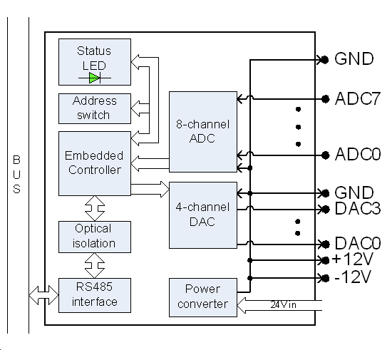
Electrical characteristics
Power :
Bus voltage:12V
Bus power consumption:100mA
Field power voltage:24V
Maximum field power consumption:500mA
Insulation :
Optical isolation voltage:2500VRMS
AD converter :
Input voltage range:5V
Input resistance:820k
Input capacitance:2nF
DA converter :
Output voltage range:10V
Maximum output current:20mA
Connection
LinuxCNC HAL configuration
All the pins and parameters are updated by the following function:
gm.<nr. of card>.rs485
It should be added to the servo thread or other thread with larger period to avoid CPU overload.
Every RS485 module pin and parameter name begins as follows:
gm.<nr. of card>.rs485.<modul ID> ,where <modul ID> is from 00 to 15.
Pins:
.adc-<0-7>(float, Out)--Value of ADC input in Volts.
.dac-enable-<0-3>(bit, In)--Enable DAC output. When enable is false DAC
output is set to 0.0 V.
.dac-<0-3>(float, In) --Value of DAC output in Volts.
Parameters:
.adc-scale-<0-7>(float, R/W)--The input voltage will be multiplied by scale before being output to .adc- pin.
.adc-offset-<0-7>(float, R/W)--Offset is subtracted from the hardware input voltage after the scale multiplier has been applied.
.dac-offset-<0-3>(float, R/W)--Offset is added to the value before the hardware is updated.
.dac-high-limit-<0-3>(float, R/W)--Maximum output voltage of the hardware in volts.
.dac-low-limit-<0-3>(float, R/W)--Minimum output voltage of the hardware in volts.
For example:
gm.0.rs485.0.adc-0 – First analogue channel of the node.
gm.0 – Means the first PCI motion control card (PCI card address = 0).
.rs485.0 – Select node with address 0 on the RS485 bus.
.adc-0 – Select the first analogue input of the module.
13.5.4. Teach pendant module
Electrical characteristics
Power:
Bus voltage:12V
Bus power consumption:100mA
Maximum load of 5V outputs:500mA
AD converter:
Input voltage range:0.5V
Input leakage current:50nA
Analogue input resistance:100MΩ
Input pin characteristics (Digital inputs and encoder inputs):
These are simple non-isolated I/O ports for general purpose usage. All voltage levels are referenced to the PC ground.
Absolute minimum input voltage:-0.5V
Absolute maximum input voltage:5.5V
Maximum low level input voltage:0.3V
Minimum high level input voltage:0.6V
Input leakage current1µA
Connection
LinuxCNC HAL configuration
All the pins and parameters are updated by the following function:
gm.<nr. of card>.rs485
It should be added to the servo thread or other thread with larger period to avoid CPU overload.
Every RS485 module pin and parameter name begins as follows:
gm.<nr. of card>.rs485.<modul ID> ,where <modul ID> is from 00 to 15.
Pins:
.adc-<0-7>(float, Out)--Value of ADC input in Volts.
.dac-enable-<0-3>(bit, In)--Enable DAC output. When enable is false DAC
output is set to 0.0 V.
.dac-<0-3>(float, In) --Value of DAC output in Volts.
Parameters:
.adc-scale-<0-7>(float, R/W)--The input voltage will be multiplied by scale before being output to .adc- pin.
.adc-offset-<0-7>(float, R/W)--Offset is subtracted from the hardware input voltage after the scale multiplier has been applied.
.dac-offset-<0-3>(float, R/W)--Offset is added to the value before the hardware is updated.
.dac-high-limit-<0-3>(float, R/W)--Maximum output voltage of the hardware in volts.
.dac-low-limit-<0-3>(float, R/W)--Minimum output voltage of the hardware in volts.
For example:
gm.0.rs485.0.adc-0 – First analogue channel of the node.
gm.0 – Means the first PCI motion control card (PCI card address = 0)
.rs485.0 – Select node with address 0 on the RS485 bus
.adc-0 – Select the first analogue input of the module
13.5.5. Mechanical dimensions
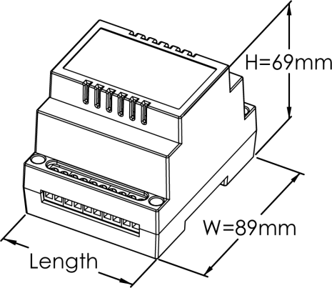
Lengths of each module:
Relay output module:139mm
Input module:65mm
ADC & DAC module:107mm
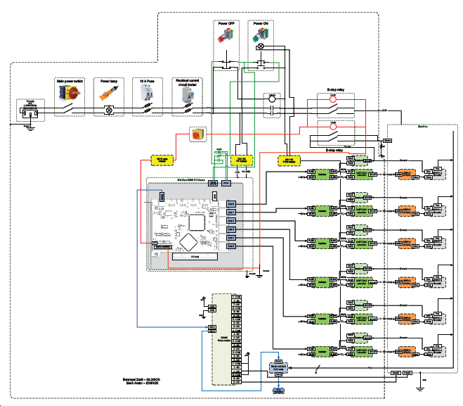
13.6. Digital Servo Drives (BMEGEMIMM25)
Homework
Select an industrial machine tool, for example CNC milling machine, CNC lathe or industrial robot. Review the corresponding literature (user’s guide, book of machine). Prepare the block diagram of the machine’s control and describe the operation of the block diagram. The project will be accepted only in the case that there are no theoretical mistakes in it. Two or three students may work on one project. In the case of three students in one project, the selected machine has to be more complex and it has to include an additional part (like tool magazine, cooling circuit, automatic door, etc.). Please consult with your instructor in the case of substantially different problem.
Signature: 7th week of lecture period, Submission deadline: 14th week of the lecture period
Students:
|
Name |
Neptun code |
Signature |
|
|
1. |
|||
|
2. |
|||
|
3. |
Selected machine:
|
Type (eg.: SCARA robot-arm) |
Manufacturer (eg.: SEIKO) |
Model noumber (eg.: D-TRAN TT 4000 SC) |
Degree of freedom (eg.: 4) |
End-effector (eg.: megfogó) |
Task description (in the case of individual project):
…………………………………………………………………………………………………………………………………………………………………………………………………………………………………………………………………………………………………………………………………………………………………………………………………………
The project is (instructor fills it out)
issued by: Name: ………………………………..... Date: .……………………...
signed: Name: ………………………………..... Date: ………………………
approved: Name: ……………………………… Date: ………………………
Grade: …………..
13.7. Robot application Homework (Sample)
13.7.1. Authors
Zsolt Baranyai
Andor Szabolcs Simó
13.7.2. Project description
Understanding of the selected machine’s control. Displaying the control’s of the block diagram. Documenting the implementation of one selected part at wiring level.
13.7.3. Selected machine
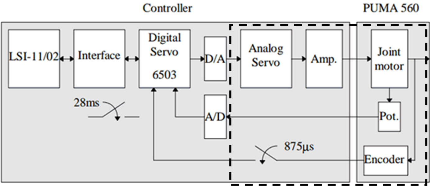
The selected machine is PUMA 560 robot. The machine has 6 degrees of freedom. There are 6 revolute joints in the robot’s structure, where the last three represent a wrist. The joints are actuated by direct current. The positioning is solved by incremental encoders, which also have an index sign. Initializations of the absolute values are obtained by using an absolute potentiometer.
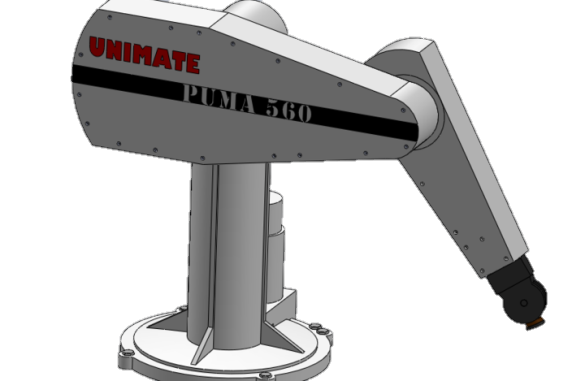
An universal gripper is chosen as the end effector of the robot. The end effector is driven by open and close logical commands. The robot brake function is also included into the model which stops the robot in case of any disturbance. This function is inegrated in the E-Stop circuit.
13.7.4. Elaboration in summary
The actuators, sensors, power amplifiers are kept the same as in original the original assembly. The analog servo is also kept thus the reference signal has to be the torque.
The communication is determined by the TTL on the side of the robot. While on the control’s side, the moduls are used for communication.
The idea is that all the additional parts are placed in a control cabinet, including the PC. Therefore common grounding can be used.
The designed block diagram is in the appendix. Where the break and the overheating events and their wiring are detailed in a schematic diagram.
The original control of the PUMA 560 is in the Figure 12-25, where the framed part is kept.
|
|
|
Figure 12-25. The original control of the PUMA 560. |
|
http://citeseerx.ist.psu.edu/viewdoc/summary?doi=10.1.1.56.815 download: 2013. november 2. Nuno Moreira et al [1996]: First Steps Towards an Open Control Architecture for a PUMA 560 |
13.7.5. Attachment
-
Block diagram of the control.
-
Breakout and DAC modules.
-
Table of the robot’s wiring and control.
Connection of the Encoder breakout and the DAC modules. More details are presented in the attached table.
13.7.6. Blockdiagram of the control
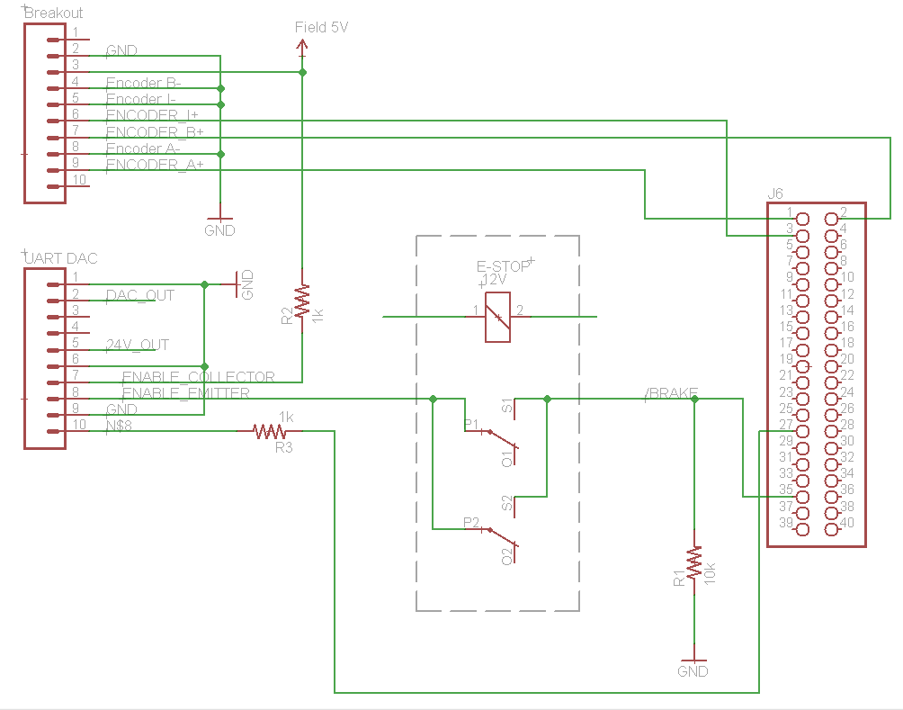
Breakout and DAC modules
|
Robot plugs |
||||||
|
J5 |
|
Place of the connection |
|
|||
|
Pin |
Name |
Modul |
Pin |
Name |
Comment |
|
|
1 |
POT_J1 |
|
RS485 ADC/DAC |
10 |
ADC-0 |
|
|
2 |
POT_J2 |
|
RS485 ADC/DAC |
11 |
ADC-1 |
|
|
3 |
POT_J3 |
|
RS485 ADC/DAC |
12 |
ADC-2 |
|
|
4 |
POT_J4 |
|
RS485 ADC/DAC |
13 |
ADC-3 |
|
|
5 |
POT_J5 |
|
RS485 ADC/DAC |
14 |
ADC-4 |
|
|
6 |
POT_J6 |
|
RS485 ADC/DAC |
15 |
ADC-5 |
|
|
7 |
POT_J7 |
|
|
NC |
|
|
|
8 |
POT_J8 |
|
|
NC |
|
|
|
9 |
ADGND |
|
|
GND |
GND |
|
|
10 |
AD+5V |
|
|
Field 5V |
Field 5V |
|
|
11 |
NC |
|
|
NC |
|
|
|
12 |
NC |
|
|
NC |
|
|
|
13 |
+12V |
|
RS485 ADC/DAC |
4 |
+12V |
|
|
14 |
+12V |
|
RS485 ADC/DAC |
4 |
+12V |
|
|
15 |
DAGND |
|
|
GND |
|
|
|
16 |
DAGND |
|
|
GND |
|
|
|
17 |
-12V |
|
RS485 ADC/DAC |
3 |
-12V |
|
|
18 |
-12V |
|
RS485 ADC/DAC |
3 |
-12V |
|
|
19 |
DAC+J1 |
|
UART/DAC 0 |
2 |
Analog out |
|
|
20 |
DAC-J1 |
|
|
GND |
GND |
|
|
21 |
DAC+J2 |
|
UART/DAC 1 |
2 |
Analog out |
|
|
22 |
DAC-J2 |
|
|
GND |
GND |
|
|
23 |
DAC+J3 |
|
UART/DAC 2 |
2 |
Analog out |
|
|
24 |
DAC-J3 |
|
|
GND |
GND |
|
|
25 |
DAC+J4 |
|
UART/DAC 3 |
2 |
Analog out |
|
|
26 |
DAC-J4 |
|
|
GND |
GND |
|
|
27 |
DAC+J5 |
|
UART/DAC 4 |
2 |
Analog out |
|
|
28 |
DAC-J5 |
|
|
GND |
GND |
|
|
29 |
DAC+J6 |
|
UART/DAC 5 |
2 |
Analog out |
|
|
30 |
DAC-J6 |
|
|
GND |
GND |
|
|
31 |
DAC+J7 |
|
|
GND |
GND |
|
|
32 |
DAC-J7 |
|
|
GND |
GND |
|
|
33 |
DAC+J8 |
|
|
GND |
GND |
|
|
34 |
DAC-J8 |
|
|
GND |
GND |
|
|
|
|
|
|
|
|
|
|
J6 |
|
|
|
|
|
|
|
1 |
ENCA1 |
|
Breakout 0 |
9 |
Encoder A+ |
|
|
2 |
ENCB1 |
|
Breakout 0 |
7 |
Encoder B+ |
|
|
3 |
ENCI1 |
|
Breakout 0 |
6 |
Encoder I+ |
|
|
4 |
ENCA2 |
|
Breakout 1 |
9 |
Encoder A+ |
|
|
5 |
ENCB2 |
|
Breakout 1 |
7 |
Encoder B+ |
|
|
6 |
ENCI2 |
|
Breakout 1 |
6 |
Encoder I+ |
|
|
7 |
ENCA3 |
|
Breakout 2 |
9 |
Encoder A+ |
|
|
8 |
ENCB3 |
|
Breakout 2 |
7 |
Encoder B+ |
|
|
9 |
ENCI3 |
|
Breakout 2 |
6 |
Encoder I+ |
|
|
10 |
ENCA4 |
|
Breakout 3 |
9 |
Encoder A+ |
|
|
11 |
ENCB4 |
|
Breakout 3 |
7 |
Encoder B+ |
|
|
12 |
ENCI4 |
|
Breakout 3 |
6 |
Encoder I+ |
|
|
13 |
ENCA5 |
|
Breakout 4 |
9 |
Encoder A+ |
|
|
14 |
ENCB5 |
|
Breakout 4 |
7 |
Encoder B+ |
|
|
15 |
ENCI5 |
|
Breakout 4 |
6 |
Encoder I+ |
|
|
16 |
ENCA6 |
|
Breakout 5 |
9 |
Encoder A+ |
|
|
17 |
ENCB6 |
|
Breakout 5 |
7 |
Encoder B+ |
|
|
18 |
ENCI6 |
|
Breakout 5 |
6 |
Encoder I+ |
|
|
19 |
GND |
|
|
GND |
GND |
|
|
20 |
GND |
|
|
GND |
GND |
|
|
21 |
Vcc |
|
|
Field 5V |
Field 5V |
|
|
22 |
Vcc |
|
|
Field 5V |
Field 5V |
|
|
23 |
NC |
|
|
NC |
NC |
|
|
24 |
NC |
|
|
NC |
NC |
|
|
25 |
NC |
|
|
NC |
NC |
|
|
26 |
/STOP |
|
|
NC |
NC |
There is a separate E-Stop. |
|
27 |
THERM1 |
|
UART/DAC 0 |
10 |
Fault Anode |
1kOhm resistance |
|
28 |
THERM2 |
|
UART/DAC 1 |
10 |
Fault Anode |
1kOhm resistance |
|
29 |
THERM3 |
|
UART/DAC 2 |
10 |
Fault Anode |
1kOhm resistance |
|
30 |
THERM4 |
|
UART/DAC 3 |
10 |
Fault Anode |
1kOhm resistance |
|
31 |
THERM5 |
|
UART/DAC 4 |
10 |
Fault Anode |
1kOhm resistance |
|
32 |
THERM6 |
|
UART/DAC 5 |
10 |
Fault Anode |
1kOhm resistance |
|
33 |
NC |
|
|
NC |
NC |
|
|
34 |
NC |
|
|
NC |
NC |
|
|
35 |
/BRAKE |
|
E-Stop Relé |
2 |
E-Stop Relé |
NO |
|
36 |
HANDO |
|
RS-485 Relay |
1 |
0-NO |
|
|
37 |
HANDC |
|
RS-485 Relay |
4 |
1-NO |
|
|
38 |
UTIL4 |
|
|
NC |
NC |
|
|
39 |
UTIL5 |
|
|
NC |
NC |
|
|
40 |
UTIL6 |
|
|
NC |
NC |
|
13.7.7. Table: Connection of the robot and the control
|
Pin |
Signal |
Backplane |
Pin |
Signal |
Backplane |
|
|
# |
Name |
Location |
# |
Name |
Location |
|
|
1 |
POT_J1 |
J56A-F1 |
18 |
-12V |
TB5-4 |
|
|
2 |
POT_J2 |
J56A-N1 |
19 |
DAC+J1 |
J103-11 |
|
|
3 |
POT_J3 |
J56A-V1 |
20 |
DAC-J1 |
J103-12 |
|
|
4 |
POT_J4 |
J56B-F1 |
21 |
DAC+J2 |
J103-13 |
|
|
5 |
POT_J5 |
J56B-N1 |
22 |
DAC-J2 |
J103-14 |
|
|
6 |
POT_J6 |
J56B-V1 |
23 |
DAC+J3 |
J103-15 |
|
|
7 |
POT_J7 |
J56B-H2 |
24 |
DAC-J3 |
J103-16 |
|
|
8 |
POT_J8 |
J56A-R2 |
25 |
DAC+J4 |
J103-17 |
|
|
9 |
ADGND |
J56A-E2 |
26 |
DAC-J4 |
J103-18 |
|
|
10 |
AD+5V |
J56A-F2 |
27 |
DAC+J5 |
J103-19 |
|
|
11 |
NC |
28 |
DAC-J5 |
J103-20 |
||
|
12 |
NC |
29 |
DAC+J6 |
J103-21 |
||
|
13 |
+12V |
TB5-3 |
30 |
DAC-J6 |
J103-22 |
|
|
14 |
+12V |
TB5-3 |
31 |
DAC+J7 |
J103-23 |
|
|
15 |
DAGND |
TB5-2 |
32 |
DAC-J7 |
J103-24 |
|
|
16 |
DAGND |
TB5-2 |
33 |
DAC+J8 |
J103-25 |
|
|
17 |
-12V |
TB5-4 |
34 |
DAC-J8 |
J103-26 |
|
|
1 |
ENCA1 |
J56A-A1 |
21 |
Vcc |
TB5-1 |
|
|
2 |
ENCB1 |
J56A-C1 |
22 |
Vcc |
TB5-1 |
|
|
3 |
ENCI1 |
J56A-E1 |
23 |
NC |
||
|
4 |
ENCA2 |
J56A-H1 |
24 |
NC |
||
|
5 |
ENCB2 |
J56A-K1 |
25 |
NC |
||
|
6 |
ENCI2 |
J56A-M1 |
26 |
/STOP |
J69-12c |
|
|
7 |
ENCA3 |
J56A-P1 |
27 |
THERM1 |
J56A-B1 |
|
|
8 |
ENCB3 |
J56A-S1 |
28 |
THERM2 |
J56A-J1 |
|
|
9 |
ENCI3 |
J56A-U1 |
29 |
THERM3 |
J56A-R1 |
|
|
10 |
ENCA4 |
J56B-A1 |
30 |
THERM4 |
J56B-B1 |
|
|
11 |
ENCB4 |
J56B-C1 |
31 |
THERM5 |
J56B-J1 |
|
|
12 |
ENCI4 |
J56B-E1 |
32 |
THERM6 |
J56B-R1 |
|
|
13 |
ENCA5 |
J56B-H1 |
33 |
NC |
||
|
14 |
ENCB5 |
J56B-K1 |
34 |
NC |
||
|
15 |
ENCI5 |
J56B-M1 |
35 |
UTIL1 |
J103-5 |
/BRAKE |
|
16 |
ENCA6 |
J56B-P1 |
36 |
UTIL2 |
J44A-M2 |
HANDO |
|
17 |
ENCB6 |
J56B-S1 |
37 |
UTIL3 |
J44A-L2 |
HANDC |
|
18 |
ENCI6 |
J56B-U1 |
38 |
UTIL4 |
SPARE1 |
|
|
19 |
GND |
TB5-2 |
39 |
UTIL5 |
SPARE2 |
|
|
20 |
GND |
TB5-2 |
40 |
UTIL6 |
SPARE3 |
|